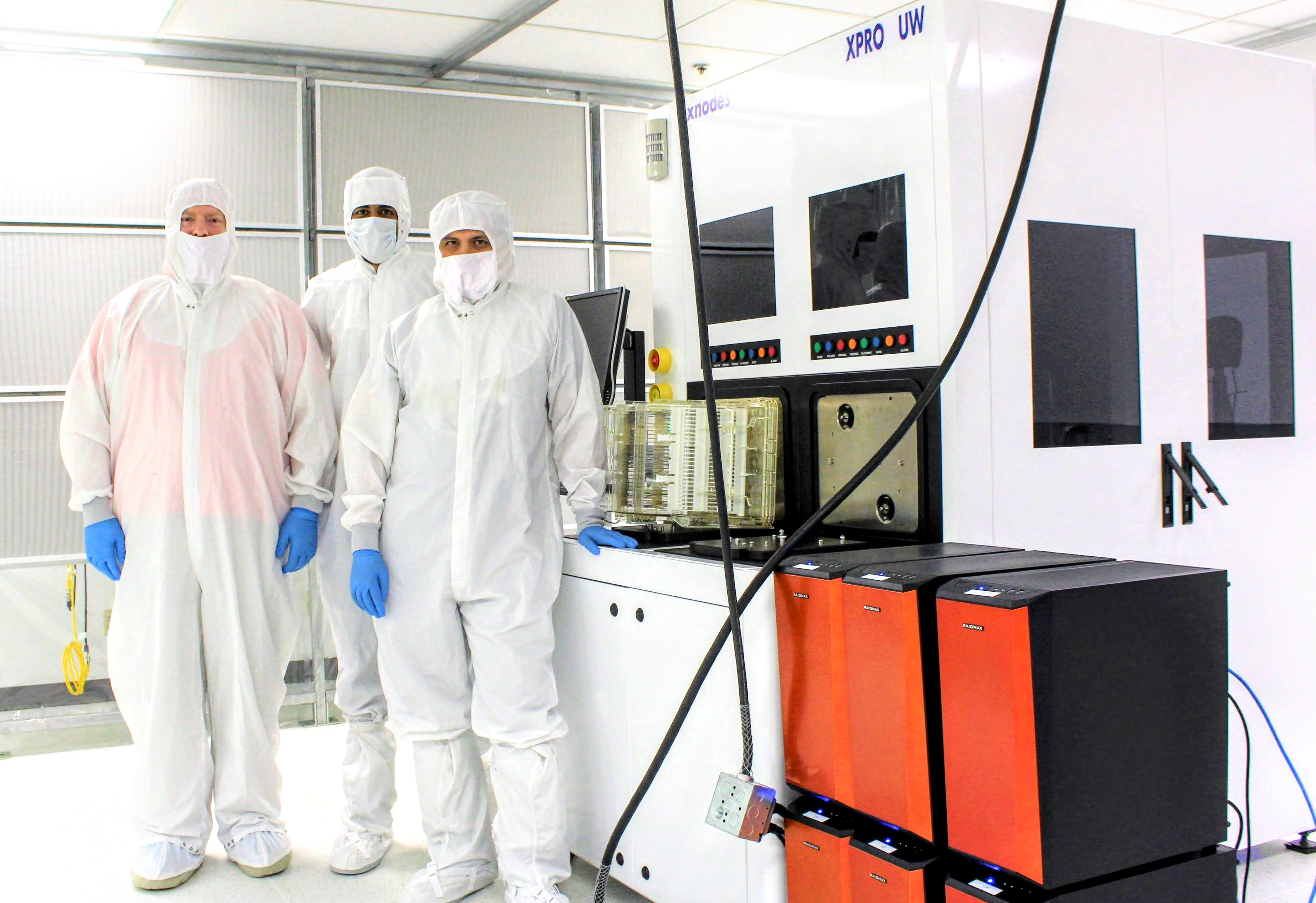
Exnodes detects 20 nm defects at 120 wph
8.9 nm sensitivity breakthrough with visible light.
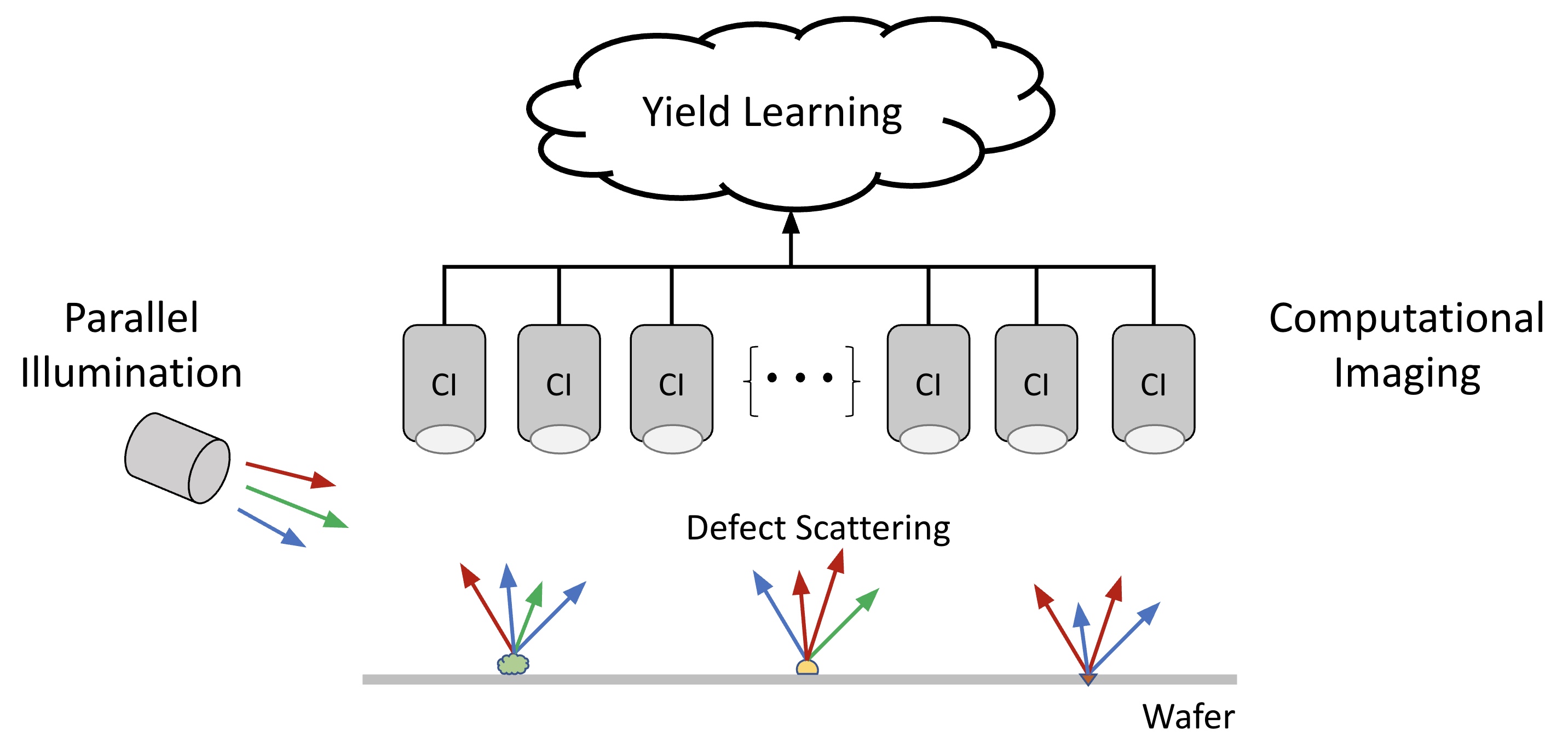
Unpatterned wafer inspection without DUV baggage.
Computational Parallel Inspection® (CPI)
- Wide illumination coverage with visible wavelengths.
- Matched detection with wide field computational imaging.
- Detection, classification & root cause analysis with AI models.
- Backed by 10 patents
Exnodes licenses technology to industry leaders in SEMI.
Accelerate your process at the leading edge.
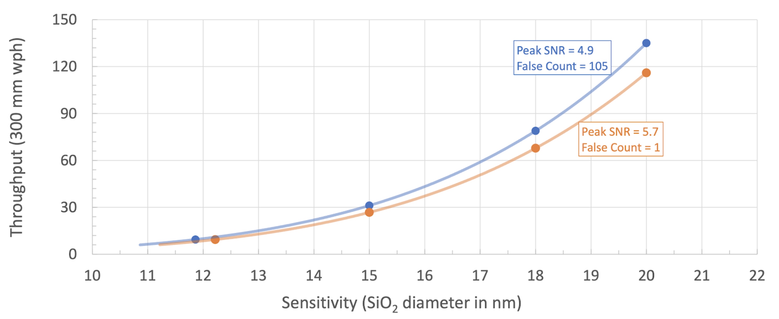
120 wph at 20 nm SiO2 sensitivity.
Real-time feedback loops in 3 nm node volume manufacturing.
Compact footprint enables onboard modules for cluster tools.
Exnodes is backed by world's leading semiconductor companies.


Simultaneous detection of 8.9 nm to 100 nm defects.
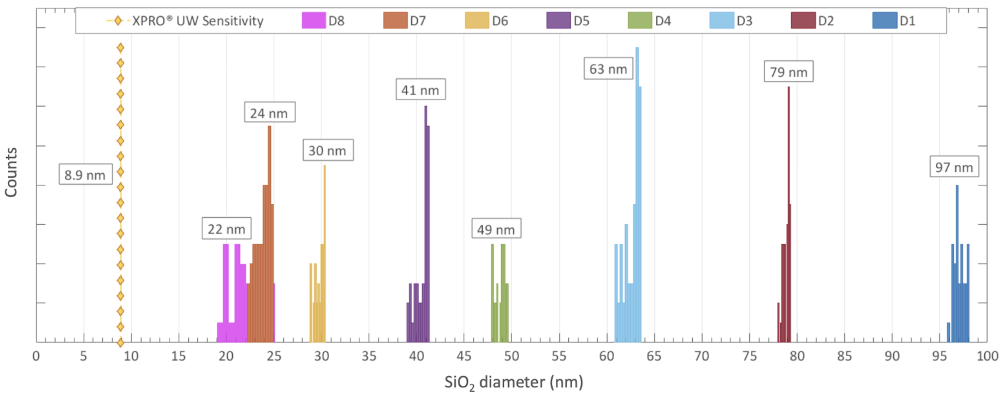
Validated by industry leaders over a wide range of defect sizes.